Giant Magneto-Resistance Devices PDF
Preview Giant Magneto-Resistance Devices
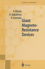
SPRINGER SERIES IN SURFACE SCIENCES 40 Springer-Verlag Berlin Heidelberg GmbH ONLINE LIBRARY Physics and Astronomy http:// www.springer.de/phys/ SPRINGER SERIES IN SURFACE SCIENCES Series Editors: G. Ertl, R. Gomer, H. Liith and D.L. Mills This series covers the whole spectrum of surface sciences, including structure and dynamics of clean and adsorbate-covered surfaces, thin films, basic surface effects, analytical methods and also the physics and chemistry of interfaces. Written by leading researchers in the field, the books are intended primarily for researchers in academia and industry and for graduate students. 38 Progress in Transmission Electron Microscopy 1 Concepts and Techniques Editors: X.-F. Zhang, Z. Zhang 39 Progress in Transmission Electron Microscopy 2 Applications in Materials Science Editors: X.-F. Zhang, Z. Zhang 40 Giant Magneto-Resistance Devices By E. Hirota, H. Sakakima, and K. Inomata 41 The Physics of Ultra-High-Density Magnetic Recording Editors: M.L. Plumer, J. van Ek, and D. Weller Series homepage-http://www.springer.de/phys/books/ssss/ Volumes 1-37 are listed at the end of the book E. Hirota H. Sakakima K. Inomata Giant Magneto-Resistance Devices With 167 Figures Springer Professor Dr. Eiichi Hirota Professor Dr. Hirosi Sakakima Advanced Technology Reserach Laboratories, Matushita Electric Industrial Co., Ltd. 3-4 Hikaridai, Seika, Souraku, Kyoto, 619-0237, Japan E-mail: e-hirota@muj.biglobe.ne.jp, sakakima@crl.mei.co.jp Professor Dr. Koichiro Inomata Department of Materials Science, Tohoku University 02 Aza-aoba, Aramaki, Aoba-ku, Sendai 980-8579, Japan E-mail: inomata@material.tohoku.ac.jp Series Editors: Professor Dr. Gerhard Ertl Fritz-Haber-Institute der Max-Planck-Gesellschaft, Faradayweg 4-6, 14195 Berlin, Germany Professor Robert Gomer, Ph.D. The James Franck Institute, The University of Chicago, 5640 Ellis Avenue, Chicago, IL 60637, USA Professor Dr. Hans Liith Institut fiir Schicht-und Ionentechnik Forschungszentrum Jiilich GmbH, 52425 Ji ilich, Germany Professor Douglas L. Mills, Ph.D. Department of Physics, University of California, Irvine, CA 92717, USA Library of Congress Cataloging-in-Publication Data applied for Die Deutsche Bibliothek -CIP-Einheitsaufnahme Hirota, Eiichi: Giant magneto-resistance devices I E. Hirota ; H. Sakakima ; K. Inomata. (Springer series in surface sciences ; 40) (Physics and astronomy library) ISBN 978-3-642-07526-1 ISBN 978-3-662-04777-4 (eBook) DOI 10.1007/978-3-662-04777-4 ISSN 0931-5195 ISBN 978-3-642-07526-1 This work is subject to copyright. All rights are reserved, whether the whole or part of the material is concerned, specifically the rights of translation, reprinting, reuse of illustrations, recitation, broadcasting, reproduction on microfilm or in any other way, and storage in data banks. Duplication of this publication or parts thereof is permitted only under the provisions of the German Copyright Law of September 9, 1965, in its current version, and permission for use must always be obtained from Springer-Verlag Berlin Heidelberg GmbH. Violations are liable for prosecution under the German Copyright Law. http://www.springer.de ©Springer-Verlag Berlin Heidelberg 2002 Originally published by Springer-Verlag Berlin Heidelberg New York in 2002 Softcover reprint of the hardcover I st edition 2002 The use of general descriptive names, registered names, trademarks, etc. in this publication does not imply, even in the absence of a specific statement, that such names are exempt from the relevant protective laws and regulations and therefore free for general use. Typesetting: Layout by author and Marianne Schillinger-Dietrich (Offsetmontagen), Berlin Cover concept: eStudio Calamar Steinen Cover production: design & production GmbH, Heidelberg Printed on acid-free paper SPIN: 10779009 57/3020/Rw-5 4 3 2 1 o Preface In the last decade after the discovery of "giant magnetoresistance effects" in me tallic multilayers worldwide developments in basic research and in engineering applications have been achieved, and various remarkable results have been ob tained in both fields. On the basic research into the GMR effects an excellent re view book edited by Hartmann was published in 1999, entitled "Magnetic Multi layers and Giant Magnetoresistance", and it describes the experimental and theoretical aspects of GMR studies and the magneto-optics in metallic multilayers, including applications in electronic data storage fields. This book aims to give an overview on the electronics applications of the GMR in metallic multilayers, espe cially on the sensors and memories in magnetic data storage, the main concerns of electronic engineers. If the mean free path of conduction electrons is longer than the period of the multilayer, and for a low applied magnetic field magnetizations in the adjacent magnetic layers are in antiparallel, the GMR effect in magnetic metallic multilay ers occurs due to the resistance change in the electric current flowing in the layer plain, with a change in the magnetization from antiparallel to parallel alignment by an applied magnetic field (CIP mode), i.e., in the saturation field magnetiza tions are in parallel and the resistance is lowered. The saturation field H, is given by the RKKY-like magnetic coupling between adjacent magnetic layers through a nonmagnetic conductive layer between the layers. In early GMR multilayers H, was larger than 0.1 T and they could not be used in electronic devices. Electronic applications need multilayer systems with low H,, such as the [NiFe/Cu/Co/Cu] multilayer with a H, of 1 mT. These low-H, systems and their sensor applications are described. After proposal of "spin valve" or "pseudo-spin-valve" techniques for novel devices, which are essentially trilayer devices composed of a nonmag netic layer sandwiched between two magnetic layers, the development research shifts to these spin-valve-type devices which are now used in the market in read heads in hard disk drives (HDDs ). This is one of the main subjects of this book. When an electric current flows perpendicular to the layer plain (CPP mode), the GMR effect becomes larger than that in the CIP mode. But devices in this mode show impedances too low for use. A practical GMR device in CPP mode is con structed by using a ferromagnetic tunnel junction (MTJ), i.e., the nonmagnetic conductive layer in the spin valve is replaced by an insulator film. This so called TMR device has high potential for future electronics applications. A probable ap plication is magnetic random access memory (MRAM) and this is another main subject in this book. The forecast for other possible spin electronics devices is also given in this book. VI Preface The purpose of this book is to provide a text on GMR devices for electronic material scientists and/or device engineers, and for graduate students in these fields, and give an overview of applications and elemental physics models related to GMR and TMR devices. The authors' backgrounds are in solid-state physics where we accumulated knowledge and experience through research and develop ment into electronic materials and devices, especially from magnetic materials and related devices. This book started with a recommendation from Dr. S. Y osimura and he intro duced us to his friend Dr. Claus E. Ascheron of Springer-Verlag. We would like to express our thanks for their continuous concern and support. Osaka, Kyoto and Sendai, Japan E. Hirota May 2001 H. Sakakima K. lnomata Contents 1 Introduction (E. Hirota) ........................................... . 1 1.1 Magnetic Transducers (Sensor and Read Head) .................... . 3 1.1.1 MR Sensor ............................................... . 4 1.1.2 HDD Head ............................................... . 5 1.2 Magnetic Random Access Memory (MRAM). . . . . . . . . . . . . . . . . . . . . . . 9 References......................................................... 10 2 Physics of GMR and TMR Devices (E. Hirota) . . . . . . . . . . . . . . . . . . . . . . . 11 2.1 Spin Pinning . . . . . . . . . . . . . . . . . . . . . . . . . . . . . . . . . . . . . . . . . . . . . . . . . . . 12 2.1.1 Phenomenological Theory of Spin Pinning . . . . . . . . . . . . . . . . . . . . 12 2.1.2 Micromagnetic Theory of Spin Pinning . . . . . . . . . . . . . . . . . . . . . . . 17 2.2 Free-Electron Model of GMR Effect . . . . . . . . . . . . . . . . . . . . . . . . . . . . . . 23 2.2.1 Conductivity of Metals and Metal Films . . . . . . . . . . . . . . . . . . . . . . 24 2.2.2 Conductivity of a Ferromagnetic Metal (Two-Current Model). . . . 26 2.2.3 Two-Current Model for the GMR Effect . . . . . . . . . . . . . . . . . . . . . . 29 2.3 Free-Electron Model of the TMR Decices . . . . . . . . . . . . . . . . . . . . . . . . . . 36 2.3.1 Simmon' Formula for the Tunnel Current. . . . . . . . . . . . . . . . . . . . . . 36 2.3.2 Ferromagnetic Tunnel Junction . . . . . . . . . . . . . . . . . . . . . . . . . . . . . . 40 References. . . . . . . . . . . . . . . . . . . . . . . . . . . . . . . . . . . . . . . . . . . . . . . . . . . . . . . . . 45 3 GMR Devices of Metallic Multilayers (H. Sakakima). . . . . . . . . . . . . . . . . . 47 3.1 Exchange Coupled Metallic Multilayers . . . . . . . . . . . . . . . . . . . . . . . . . . . 47 3.1.1 Interlayer Coupling in Metallic Multilayers .................... 47 3.1.2 MR Properties of Metallic Multilayers . . . . . . . . . . . . . . . . . . . . . . . . 51 3.1.3 Dependence of the MR Properties on the Film Structures. . . . . . . . 55 3.1.4 Thermal Stability of the MR Ratios. . . . . . . . . . . . . . . . . . . . . . . . . . . 62 3.2 Magnetic Sensors ............................................... 65 3.2.1 Static Characteristics . . . . . . . . . . . . . . . . . . . . . . . . . . . . . . . . . . . . . . . 65 3.2.2 Dynamic Characteristics . . . . . . . . . . . . . . . . . . . . . . . . . . . . . . . . . . . . 67 References ......................................................... 70 4 Spin-Valve Devices (H. Sakakima) ................................... 72 4.1 Spin Valves ................................................... 72 4.1.1 Exchange-Biased Spin Valves ............................... 72 4.1.2 Pseudo-Spin-Valves. . . . . . . . . . . . . . . . . . . . . . . . . . . . . . . . . . . . . . . . 77 4.2 Enhancement of GMR. . . . . . . . . . . . . . . . . . . . . . . . . . . . . . . . . . . . . . . . . . . 80 4.2.1 Back-Layer Effect . . . . . . . . . . . . . . . . . . . . . . . . . . . . . . . . . . . . . . . . . 80 4.2.2 Specular Scattering Effect. . . . . . . . . . . . . . . . . . . . . . . . . . . . . . . . . . . 83 VIII Contents 4.3 Magnetic Read Heads........................................... 99 4.3.1 Head Design .............................................. 100 4.3.2 Spin Valves for Read Heads . . . . . . . . . . . . . . . . . . . . . . . . . . . . . . . . 106 References . . . . . . . . . . . . . . . . . . . . . . . . . . . . . . . . . . . . . . . . . . . . . . . . . . . . . . . . 111 5 Tunnel-Type GMR (TMR) Devices (K Inomata and H. Sakakima) . . . . 115 5.1 Spin-Dependent Tunneling ...................................... 115 5 .1.1 Tunneling Magnetoresistance . . . . . . . . . . . . . . . . . . . . . . . . . . . . . . . 115 5.1.2 Fabrication of Spin Tunneling Junctions. . . . . . . . . . . . . . . . . . . . . . 120 5.1.3 Microfabrication of Spin Tunneling Junctions. . . . . . . . . . . . . . . . . 122 5.1.4 Annealing Properties ....................................... 124 5.1.5 Temperature Dependence ofTMR ........................... 125 5.1.6 Bias Voltage Dependence ofTMR ........................... 127 5.1.7 Double Tunneling Junctions ................................ 129 5.2 Magnetic Read Heads ofTMR ................................... 131 References . . . . . . . . . . . . . . . . . . . . . . . . . . . . . . . . . . . . . . . . . . . . . . . . . . . . . . . . 134 6 Magnetic Random Access Memory (MRAM) (K. Inomata) . . . . . . . . . . . 135 6.1 MRAM Devices and their Operation . . . . . . . . . . . . . . . . . . . . . . . . . . . . . . 135 6.1.1 Early MRAM Devices . . . . . . . . . . . . . . . . . . . . . . . . . . . . . . . . . . . . . 135 6.1.2 MRAM Devices Using GMR Cells . . . . . . . . . . . . . . . . . . . . . . . . . . 136 6.1.3 MRAM Devices Using MTJ Cells ........................... 138 6.2 MRAM Architectures Using MTJ . . . . . . . . . . . . . . . . . . . . . . . . . . . . . . . . 138 6.3 Features ofMRAM ............................................. 140 6.4 Design of a MTJ Element ....................................... 141 6.5 Spin Switching Field for MTJ Elements ........................... 145 6.5.1 Single-Domain Calculation ................................. 145 6.5.2 Micromagnetic Simulation ................................. 146 6.5.3 Two-Dimensional Magnetic Switching. . . . . . . . . . . . . . . . . . . . . . . 148 6.6 Problems in Fabricating MRAM ................................. 151 6.6.1 Integrated Circuit Compatibility ............................. 151 6.6.2 Uniformity ofMTJ Elements ............................... 151 6. 7 Current Trial of MRAM Fabrication . . . . . . . . . . . . . . . . . . . . . . . . . . . . . . 151 6.8 Scalability ofMRAM: Challenges for High Bit Density ............. 153 6.8.1 Resistance ................................................ 153 6.8.2 Signal Voltage............................................ 153 6.8.3 Writing Current. . . . . . . . . . . . . . . . . . . . . . . . . . . . . . . . . . . . . . . . . . . 154 6.8.4 Superparamagnetism. . . . . . . . . . . . . . . . . . . . . . . . . . . . . . . . . . . . . . . 156 References . . . . . . . . . . . . . . . . . . . . . . . . . . . . . . . . . . . . . . . . . . . . . . . . . . . . . . . . 157 7 Other GMR Devices (K. Inomata) . . . . . . . . . . . . . . . . . . . . . . . . . . . . . . . . . . 158 7.1 Bipolar Spin Transistor . . . . . . . . . . . . . . . . . . . . . . . . . . . . . . . . . . . . . . . . . 158 7.1.1 Spin Injection ............................................. 158 7 .1.2 Spin Transistor Operation . . . . . . . . . . . . . . . . . . . . . . . . . . . . . . . . . . 159 7.1.3 Device Properties ......................................... 162 7 .1.4 Demonstration of a Prototype Device . . . . . . . . . . . . . . . . . . . . . . . . 162 7.2 Spin FET ...................................................... 164 Contents IX 7.3 Spin-Valve Transistor ........................................... 165 7.3.1 Principle of the Spin-Valve Transistor ........................ 165 7.3.2 Device Properties .......................................... 167 7.4 Spin-Dependent Single-Electron Tunneling Devices ................. 168 7 .4.1 Structures and Properties .................................... 168 7.4.2 TMR Enhancement by Coulomb Blockade Effect .............. 174 7.4.3 Spin Accumulation ......................................... 175 References ......................................................... 176 1 Introduction The discovery of the giant magnetoresistance (GMR) effect in metal multilayers make a strong impact on scientific researchs and also the applied sciences, espe cially on the development of computer memory technologies. The former is to re search the origin of this extraordinary large MR effect in artificial materials, such as, metal multilayers. The latter is the possibility of achieving high-density mem ory in hard disk drives (HDD) of computer peripherals. At present the introduction of GMR read heads in the HDD opens the door to the "Gb/in2 memory era" and allows aerial recording densities (ARD) of up to 100 Gb/in2• In 1971 Hunt [1] proposed using a magnetoresistance transducer, i.e., MR read heads and sensors. After his proposal various studies on MR transducers were car ried out aiming to develop practical devices. Early devices were composed with anisotropic ferromagnetic thin films, such as Fe2~i80 alloy film, which have a magnetoresistance (MR) ratio of about 2 % and which were later called aniso tropic magnetoresistance (AMR) films as distinct from GMR films. Several AMR devices were put on the market as magnetometric positioning sensors, rotary en coders, and read heads of digital audio tape recorders etc. By the beginning of the 1990 inductive thin film heads and thin film MR read heads had been put on the HDD market, successively, and attained an ARD of 1 Gb/in2 (see Fig. 1.5). Under these circumstances the GMR effect, which shows a MR ratio larger than 10 %, is very attractive as an application ofread heads to HDD. Intensive studies of this application have been done in USA, Europe and Japan. Now, GMR heads of 50 Gb/in2 have been announced and in the near future are sure to be put on the market. Successful results in GMR devices act as an incentive to study MR effects in ferromagnetic tunnel junctions (TMR), which has a MR ratio larger than 20 %. The TMR head is expected to be the next generation of read heads of HDD with an ARD of over 100 Gb/in2• The most promising TMR device is the magnetic ran dom access memory (MRAM) and many studies are now progressing with the aim of developing random access memories with high-frequency access, are nonvola tile, have low power consumption and are radiation resistant. GMR and TMR devices have a basic structure of two magnetic layers separated by a nonmagnetic spacer layer. These effects are the change in electric resistance of this basic structure, when the magnetizations of both magnetic layers change from a parallel configuration to an antiparallel configuration and vice versa, fol lowed with an applied magnetic field. Thus, the key technologies are to fabricate an antiparallel configuration, which is easily converted to a parallel configuration by a small applied field. There are two different methods: one is to use the spin- E. Hirota et al., Giant Magneto-Resistance Devices © Springer-Verlag Berlin Heidelberg 2002
The list of books you might like

A Thousand Boy Kisses

Mind Management, Not Time Management

Do Epic Shit

The 48 Laws of Power

Risk Factors in Depression
Viola silicestris, a new species in Viola section Erpetion from Australia
C Sharp How To Program
The Bunjil L6 (S4) ordinary chondrite, a new meteorite find from Western Australia

Lenoir-Rhyne College General Catalog 2006-2007

Minimalist Living: Decluttering for Joy, Health, and Creativity

The Annotated Big Sleep

Gluten-Free Bread

Tafseer E Fahm E Quran Vol 1

Beating the Street

Les Perles Sunnites dans les trésors de la Croyance

2005 Missouri State Highway System Traffic Accident Statistics

300

2006-2007 Bulletin AMENDMENT I

Atlantida

Indian Archaeology 1978-79 A Review - Archaeological Survey of

Caietele CNSAS
