NASA Technical Reports Server (NTRS) 19920012403: In-situ integrated processing and characterization of thin films of high temperature superconductors, dielectrics and semiconductors by MOCVD PDF
Preview NASA Technical Reports Server (NTRS) 19920012403: In-situ integrated processing and characterization of thin films of high temperature superconductors, dielectrics and semiconductors by MOCVD
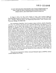
N92-21646 IN-SITU INTEGRATED PROCESSING AND CHARACTERIZATION OF THIN FILMS OF HIGH TEMPERATURE SUPERCONDUCTORS, DIELECTRICS AND SEMICONDUCTORS BY MOCVD R. Singh, S. Sinha, N.J. Hsu, R.P.S. Thakur, P. Chou, and A. Kumar, School of Electrical Engineering and Computer Science, University of Oklahoma, Norman, OK, 73019 and J. Narayan, Materials Science and Engineering Department, North Carolina State University, Raleigh, NC 27695-7916 Low temperature deposition, high throughput, sharp interfaces, selective deposition with direct ion, electron, and photon beam controlled techniques, and deposition in con- ventional as well as atomic layer epitaxy mode are some of the attractive features of MOCVD. In addition to the well established role in semiconductor and optoelectronics industry, MOCVD is expected to play a significant role in high temperature supercon- ductor industry. High temperature superconducting thin films as well as semiconductors and/or dielectrics are essentially required for the fabrication of superconductor and hy- brid superconductor/semiconductor devices. From materials compatibility point of view, the interface between two disimilar materials (e.g.superconductor/dielectric, semiconduc- tor/dielectric, etc.) should have chemical, physical, and thermal integrity during and after the processing of materials. In our strategity of depositing the basic building blocks of su- perconductors, semiconductors, and dielectric having common elements, we have deposited superconducting films of Y-Ba-Cu-O, semiconductor films of Cu20, and dielectric films of BaF2 and Y20a by MOCVD. By switching source materials entering the chamber, and by using direct writting capability complex device structure like three terminal hybrid semiconductors/superconductors transistors can be fabricated. The Y-Ba-Cu-O super- conducting thin films on BaF2/YSZ substrates show a Tc of 80K and are textured with most of the grains having their c - axis or a - axis perpendicular to the substrate. In this paper, we will report electrical characteristics as well as structural characteristics of superconductors and related materials obtained by X-ray deffraction, SEM, TEM, and energy dispersive X-ray analysis. This work was supported by Defense Advanced Research Agency (DARPA) contract number MDA972-88-D-0004 317
