Low Voltage Analog Circuit Design Techniques: A Tutorial PDF
Preview Low Voltage Analog Circuit Design Techniques: A Tutorial
Low Voltage Analog Circuit Design Techniques: A Tutorial IEEE Dallas CAS Workshop 2000 March 27, 2000 Edgar Sánchez-Sinencio http://amsc.tamu.edu/ Texas A&M University Analog and Mixed-Signal Center Low Voltage Analog Circuit Design Techniques: Roadmap Low voltage (LV) power supply circuit design techniques are addressed in this tutorial. In particular: (i) Introduction; (ii) Transistor models capable to provide performance and power consumption tradeoffs; (iii) Low voltage implementation techniques, such as floating gates and bulk driven; (iv) Basic building blocks not involving cascode structures, and (v) LV circuit implementations examples. Analog and Mixed-Signal Center, TAMU Motivation The need for analog circuits in modern mixed-signal VLSI chips for multimedia, perception, control, instrumentation medical electronics and telecommunication is very high. • What are the challenges in designing low voltage circuits ? - To operate with power supplies smaller than 3.3 volts - To design circuits with the same performance or better than circuits designed for larger power supplies - To perform with technologies smaller than 0.5 micron -To come with new design alternatives, Analog and Mixed-Signal Center, TAMU ) ( continues • Why are we concerned in designing low voltage circuits ? - Designers can not use conventional cascode structures, and other conventional design methodologies. - Circuits should have the same performance or better than circuits designed for larger power supplies - Circuit performance with technologies smaller than 0.5um must be better than circuits for larger technologies. -Third-generation communication applications require circuits ( and systems) with improved dynamic range over a much wider bandwidth. - New building blocks and system must be designed to satisfy the needs of portable, lighter and faster equipment Analog and Mixed-Signal Center, TAMU Issues about low power supply voltage Scaling down size technology and supply voltage does not scale linearly the “ V hat ” TH V TH V TH Mister 5 volts IC Mister 0.8 volts IC • Threshold and V do not scale down linearly with power DSAT supply nor with smaller size technologies. • Let us consider an illustrative example of a cascode and a simple inverting amplifiers, assume transistors MC and MS carry the same current IL, VT= 0.75V and VDS(SAT)=0.2V • Keeping the same output voltage swing for both circuits involve the tradeoffs shown in the plot of transistor sizes and GBW vs. Power Supply Voltage • How to determine how much bias current is needed for certain application ? • When a designer operates transistors in saturation, what does it mean VDS > VDS(SAT) ? • Can a circuit have their transistors operating in the transition region ? What transistor model equation can be employed ? One Equation-All Regions Transistor Model • Features of ACM model: – physics-based model, – universal and continuous expression for any inversion, – independent of technology, temperature, geometry and gate voltage, – same model for analysis, characterization and design. • Main design equations: (design parameters: I, g , i ) m f I (cid:190) drain current in transistor I 1 + 1 + i f = g (cid:190) transconductance in saturation f g n 2 m t m n (cid:190) slope factor mf ( ) f = t 2 1+ i - 1 f (cid:190) thermal voltage T 2pL2 f t i (cid:190) inversion level of the transistor defined as f W g 1 = m i = I I , where f2 W L mC f 1+ i - 1 f s I = mnC t ox t f is the normalization current. s ox 2 L V ( ) DSAT @ 1+i - 1 + 4 f i << 1 (cid:190) weak inversion, f t f W g i >> 1 (cid:190) strong inversion. = m f L (cid:230) I (cid:246) 2mC f (cid:231)(cid:231) - 1(cid:247)(cid:247) ox tŁ f g n ł t m
The list of books you might like

The Strength In Our Scars

As Good as Dead

Corrupt (Devil's Night #1)

Rich Dad Poor Dad

Bioinformatics for Everyone

Lars Gustaf Andersson 2012-01-13
Persistent entanglement due to helicity conservation in excitable media
DTIC ADA443237: Interdisciplinary Research Project to Explore the Potential for Developing Non-Lethal Weapons Based on Radiofrequency/Microwave Bioeffects

300

2006-2007 Bulletin AMENDMENT I
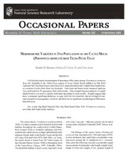
Morphometric variation in two populations of the cactus mouse (Peromyscus eremicus) from Trans-Pecos Texas
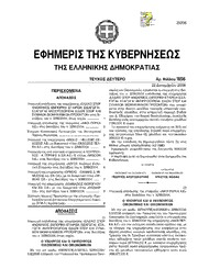
Greek Government Gazette: Part 2, 2006 no. 1856

CA APM 10 機能紹介資料
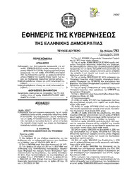
Greek Government Gazette: Part 2, 2006 no. 1783
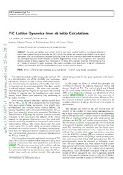
TiC lattice dynamics from ab initio calculations

by Andy Farnell

New Moon

Soul Seeking

Keeping up With William by Irving Bacheller

