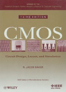
CMOS: Circuit Design, Layout, and Simulation; 3rd Edition (IEEE Press Series on Microelectronic Systems) PDF
Preview CMOS: Circuit Design, Layout, and Simulation; 3rd Edition (IEEE Press Series on Microelectronic Systems)
Contents Cover Half Title Page Title Page Copyright Dedication Preface Chapter 1: Introduction to CMOS Design 1.1 The CMOS IC Design Process 1.2 CMOS Background 1.3 An Introduction to SPICE Chapter 2: The Well 2.1 Patterning 2.2 Laying Out the N-well 2.3 Resistance Calculation 2.4 The N-well/Substrate Diode 2.5 The RC Delay through an N-well 2.6 Twin Well Processes Chapter 3: The Metal Layers 3.1 The Bonding Pad 3.2 Design and Layout Using the Metal Layers 3.3 Crosstalk and Ground Bounce 3.4 Layout Examples Chapter 4: The Active and Poly Layers 4.1 Layout using the Active and Poly Layers 4.2 Connecting Wires to Poly and Active 4.3 Electrostatic Discharge (ESD) Protection Chapter 5: Resistors, Capacitors, MOSFETs 5.1 Resistors 5.2 Capacitors 5.3 MOSFETs 5.4 Layout Examples Chapter 6: MOSFET Operation 6.1 MOSFET Capacitance Overview/Review 6.2 The Threshold Voltage 6.3 IV Characteristics of MOSFETs 6.4 SPICE Modeling of the MOSFET 6.5 Short-Channel MOSFETs Chapter 7: CMOS Fabrication 7.1 CMOS Unit Processes 7.2 CMOS Process Integration 7.3 Backend Processes 7.4 Summary Chapter 8: Electrical Noise: An Overview 8.1 Signals 8.2 Circuit Noise 8.3 Discussion Chapter 9: Models for Analog Design 9.1 Long-Channel MOSFETs 9.2 Short-Channel MOSFETs 9.3 MOSFET Noise Modeling Chapter 10: Models for Digital Design 10.1 The Digital MOSFET Model 10.2 The MOSFET Pass Gate 10.3 A Final Comment Concerning Measurements Chapter 11: The Inverter 11.1 DC Characteristics 11.2 Switching Characteristics 11.3 Layout of the Inverter 11.4 Sizing for Large Capacitive Loads 11.5 Other Inverter Configurations Chapter 12: Static Logic Gates 12.1 DC Characteristics of the NAND and NOR Gates 12.2 Layout of the NAND and NOR Gates 12.3 Switching Characteristics 12.4 Complex CMOS Logic Gates Chapter 13: Clocked Circuits 13.1 The CMOS TG 13.2 Applications of the Transmission Gate 13.3 Latches and Flip-Flops 13.4 Examples Chapter 14: Dynamic Logic Gates 14.1 Fundamentals of Dynamic Logic 14.2 Clocked CMOS Logic Chapter 15: VLSI Layout Examples 15.1 Chip Layout Chapter 16: Memory Circuits 16.1 Array Architectures 16.2 Peripheral Circuits 16.3 Memory Cells Chapter 17: Sensing Using ΔΣ Modulation 17.1 Qualitative Discussion 17.2 Sensing Resistive Memory 17.3 Sensing in CMOS Imagers Chapter 18: Special Purpose CMOS Circuits 18.1 The Schmitt Trigger 18.2 Multivibrator Circuits 18.3 Input Buffers 18.4 Charge Pumps (Voltage Generators) Chapter 19: Digital Phase-Locked Loops 19.1 The Phase Detector 19.2 The Voltage-Controlled Oscillator 19.3 The Loop Filter 19.4 System Considerations 19.5 Delay-Locked Loops 19.6 Some Examples Chapter 20: Current Mirrors 20.1 The Basic Current Mirror 20.2 Cascoding the Current Mirror 20.3 Biasing Circuits Chapter 21: Amplifiers 21.1 Gate-Drain-Connected Loads 21.2 Current Source Loads 21.3 The Push-Pull Amplifier Chapter 22: Differential Amplifiers 22.1 The Source-Coupled Pair 22.2 The Source Cross-Coupled Pair 22.3 Cascode Loads (The Telescopic Diff-Amp) 22.4 Wide-Swing Differential Amplifiers Chapter 23: Voltage References 23.1 MOSFET-Resistor Voltage References 23.2 Parasitic Diode-Based References Chapter 24: Operational Amplifiers I 24.1 The Two-Stage Op-Amp 24.2 An Op-Amp with Output Buffer 24.3 The Operational Transconductance Amplifier (OTA) 24.4 Gain-Enhancement 24.5 Some Examples and Discussions Chapter 25: Dynamic Analog Circuits 25.1 The MOSFET Switch 25.2 Fully-Differential Circuits 25.3 Switched-Capacitor Circuits 25.4 Circuits Chapter 26: Operational Amplifiers II 26.1 Biasing for Power and Speed 26.2 Basic Concepts 26.3 Basic Op-Amp Design 26.4 Op-Amp Design Using Switched-Capacitor CMFB Chapter 27: Nonlinear Analog Circuits 27.1 Basic CMOS Comparator Design 27.2 Adaptive Biasing Chapter 28: Data Converter Fundamentals 28.1 Analog Versus Discrete Time Signals 28.2 Converting Analog Signals to Digital Signals 28.3 Sample-and-Hold (S/H) Characteristics 28.4 Digital-to-Analog Converter (DAC) Specifications 28.5 Analog-to-Digital Converter (ADC) Specifications 28.6 Mixed-Signal Layout Issues Chapter 29: Data Converter Architectures 29.1 DAC Architectures 29.2 ADC Architectures Chapter 30: Implementing Data Converters 30.1 R-2R Topologies for DACs 30.2 Op-Amps in Data Converters 30.3 Implementing ADCs Chapter 31: Feedback Amplifiers 31.1 The Feedback Equation 31.2 Properties of Negative Feedback on Amplifier Design 31.3 Recognizing Feedback Topologies 31.4 The Voltage Amp (Series-Shunt Feedback) 31.5 The Transimpedance Amp (Shunt-Shunt Feedback) 31.6 The Transconductance Amp (Series-Series Feedback) 31.7 The Current Amplifier (Shunt-Series Feedback) 31.8 Stability 31.9 Design Examples Index About the Author Square-Law Equations For a triode-operating long-channel NMOS device For a long-channel NMOS device operating in the saturation region: On the border between saturation and triode: V = V – V and the drain DS,sat GS THN current is called I , see Fig. 6.11 D,sat For the PMOS device equations make the following substitutions in the equations listed above V → V , V → V , and V → V . DS SD GS SG THN THP All of the voltages and currents in the PMOS and NMOS equations are positive. For example, for the PMOS device to conduct a drain current requires V > V . SG THP For the NMOS to conduct a drain current requires V > V . GS THN
Description: